- 您现在的位置:买卖IC网 > Sheet目录2007 > LV5609LP-TE-L-E (ON Semiconductor)IC CLOCK DRIVER VERT VCT24
LV5609LP
No.A0692-4/8
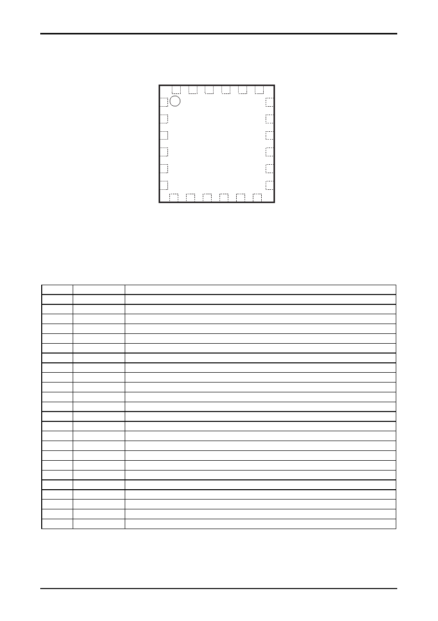
Pin Assignment
Pin Function
Pin No.
Name
Mode
1
VL
Lo power for output (-7.5V system)
2
SHT
Level shift output (binary VH, VL)
3
V4
Level shift output (binary VM, VL)
4
V3
Level shift output (ternary VH, VM, VL)
5
V2
Level shift output (binary VM, VL)
6
V1
Level shift output (ternary VH, VM, VL)
7
VM
GND for output
8
NC
9
VH
Hi power supply for output (15V system)
10
NC
11
NC
12
XV1
V1 transfer pulse input
13
XSG1
V1 read pulse input
14
XV2
V2 transfer pulse input
15
XV3
V3 transfer pulse input
16
XSG3
V3 read pulse input
17
XV4
V4 transfer pulse input
18
XSHT
SHT pulse input
19
NC
20
VDD
Power supply for input buffer (3.3V system)
21
VSS
GND for input buffer
22
NC
23
NC
24
NC
1
2
3
4
5
6
7
8
9
10
11
12
18
17
16
15
14
13
24
23
22
21
20
19
VL
SHT
V4
V3
V2
V1
VM
NC
VH
NC
XV1
XSG1
XV2
XV3
XSG3
XV4
XSHT
NC
V
DD
V
SS
NC
Top view
发布紧急采购,3分钟左右您将得到回复。
相关PDF资料
M-986-2A1PL
IC TRANSCEIVER MF 2CHAN 44-PLCC
MAX038CWP+
IC GEN WAVEFORM HI-FREQ 20-SOIC
MAX1002CAX+T
IC ADC 6BIT 60MSPS DUAL 36-SSOP
MAX1003CAX
IC ADC DUAL 6-BIT 90MSPS 36-SSOP
MAX1011CEG+
IC ADC 6BIT 90MSPS 24-QSOP
MAX105ECS+T
IC ADC 6BIT 800MSPS DL 80TQFP
MAX1063AEEG+
IC ADC 10BIT 250KSPS 24-QSOP
MAX107ECS+
IC ADC 6BIT 400MSPS DL 80-TQFP
相关代理商/技术参数
LV5609V
制造商:SANYO 制造商全称:Sanyo Semicon Device 功能描述:Bi-CMOS LSI For CCD Vertical Clock Driver
LV5609V-HAS-TLM-E
功能描述:时钟驱动器及分配 RoHS:否 制造商:Micrel 乘法/除法因子:1:4 输出类型:Differential 最大输出频率:4.2 GHz 电源电压-最大: 电源电压-最小:5 V 最大工作温度:+ 85 C 封装 / 箱体:SOIC-8 封装:Reel
LV5609V-MPB-E
功能描述:时钟驱动器及分配 RoHS:否 制造商:Micrel 乘法/除法因子:1:4 输出类型:Differential 最大输出频率:4.2 GHz 电源电压-最大: 电源电压-最小:5 V 最大工作温度:+ 85 C 封装 / 箱体:SOIC-8 封装:Reel
LV5609V-TLM-E
功能描述:时钟驱动器及分配 RoHS:否 制造商:Micrel 乘法/除法因子:1:4 输出类型:Differential 最大输出频率:4.2 GHz 电源电压-最大: 电源电压-最小:5 V 最大工作温度:+ 85 C 封装 / 箱体:SOIC-8 封装:Reel
LV-560M2W---2025S
制造商:Surge Components Inc 功能描述:CAP ALUM 56UF 450V ?20% 2000LHRS 20 X 25 - Bulk
LV560MCRO
制造商:未知厂家 制造商全称:未知厂家 功能描述:Analog IC
LV560PLID
制造商:未知厂家 制造商全称:未知厂家 功能描述:Analog IC
LV-561M2G---3545S
制造商:Surge Components Inc 功能描述:CAP ALUM 560UF 400V ?20% 2000LHRS 35 X 45 - Bulk